
Ghent, Belgium - March 16, 2026
Luceda Photonics today announced the release of Luceda Photonics Design Platform 2026.03, introducing powerful new verification and simulation capabilities that bring manufacturability and circuit validation closer to the design phase than ever before. With the launch of Luceda DRC, a new integrated, easy-to-use design rule checking (DRC) tool, dummy filling enhancements, a SPICE-based circuit simulation workflow, and improved visual placement & routing (P&R) assistance, this release empowers PIC designers to move from design to tape-out with greater confidence, transparency, and efficiency.
Key Highlights:
1. Luceda DRC – Integrated, Easy-to-Use Design Rule Checking
Introducing Luceda DRC, a native DRC engine fully integrated into the Luceda Photonics Design Platform. Designers can now detect and resolve DRC issues early, directly within their design environment, with just a few clicks. Developed to verify PIC layouts for foundry compliance, Luceda DRC brings verification closer to your design phase, significantly reduces surprises right before tape-out, and shortens the path to fabrication-ready PICs.
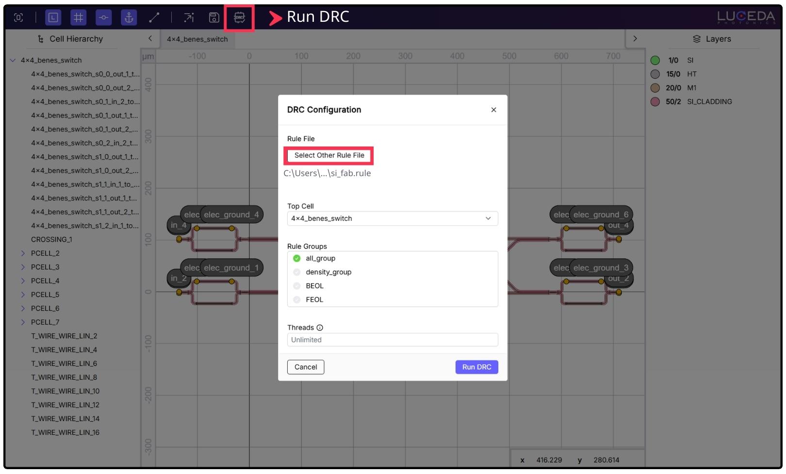 Running Luceda DRC from the Luceda Layout Visualizer.
 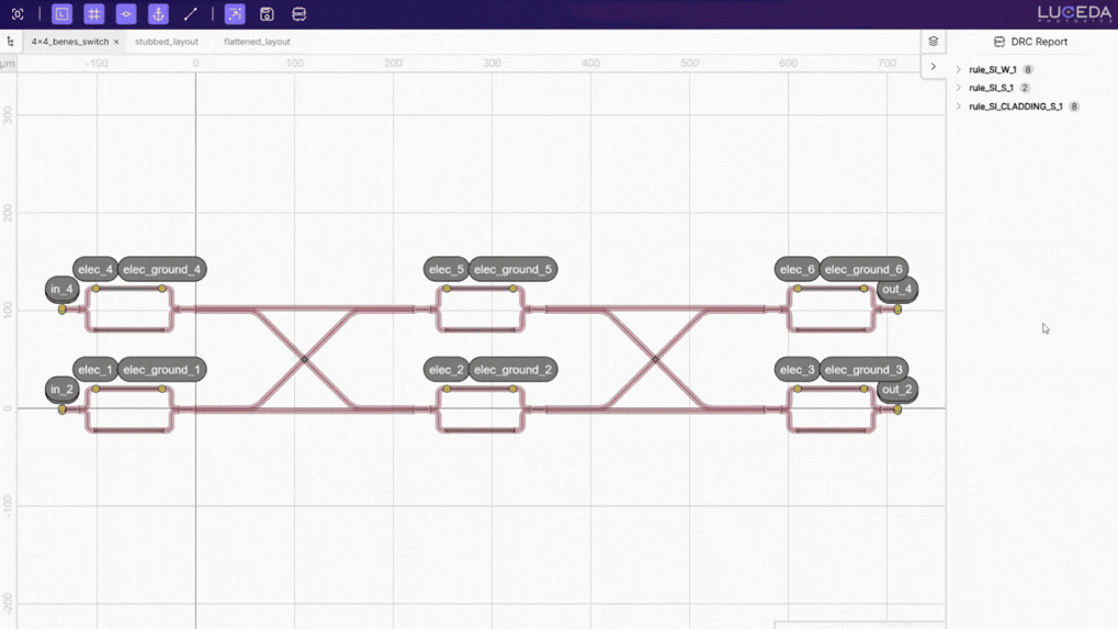 Browsing the DRC report in the Luceda Layout Visualizer.
 Key features include:
- Integrated workflow – Run DRC directly from the Luceda Layout Visualizer for immediate feedback on your PIC layout or use Python scripting for automated GDSII-based regression testing.
- Rule selection – Filter by selected rule groups (e.g., metal layers, density, BEOL, or FEOL) to manage computational load and resolve issues in complex designs.
- Cell selection – Perform DRC on the entire design, or target specific subcells to run faster, targeted checks on smaller layout sections.
- Built-in density checks – Leverage new advanced dummy filling capabilities to automatically perform density checks according to foundry specifications.
- Multi-threaded execution – Accelerate verification on large-scale layouts while keeping control over system resource allocation.
- Standardized output – Generate “.lyrdb” marker files for inspection in an external layout viewer tool such as KLayout.
Luceda Photonics is proud to collaborate with leading foundries supporting Luceda DRC, including Advanced Micro Foundry, LIGENTEC, SilTerra, and Tower Semiconductor. This collaboration helps streamline the process from design to manufacturing, enables successful tape-outs, and strengthens the PIC ecosystem. For the most up-to-date list of supported foundry DRC decks, visit: Luceda DRC
To learn how to run DRC on your designs, see the following tutorial: Luceda DRC Tutorial
2. Streamlined Tape-Out Preparation with Advanced Dummy Filling
Tape-out preparation in Luceda is now more flexible and powerful with the enhanced dummy filling functionality, i3.Filler. This new functionality enables simultaneous multi-layer dummy filling with independent settings for different layers. In addition, you can now execute a secondary dummy fill step on an already dummy-filled layout using different settings or geometries.
Dummy filling remains available for both:
- Layout Views via i3.dummy_fill_layout for applying fill directly to an IPKISS Layout while designing.
- GDSII files via i3.dummy_fill_gdsii for post-processing existing GDSII files.
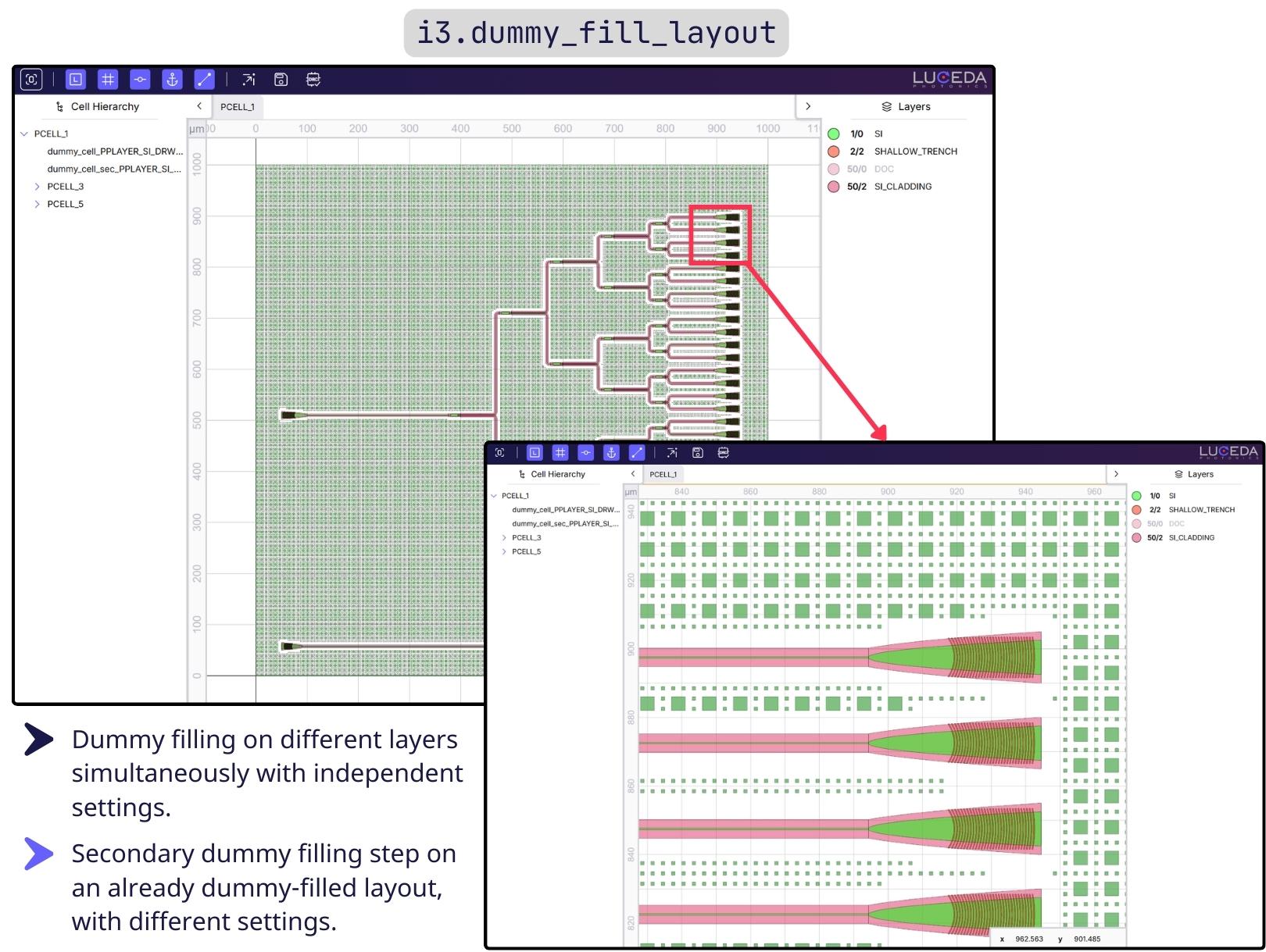
Dummy filling a layout using the new Luceda dummy filling functionality.
3. SPICE-Based Circuit Simulation – Greater Transparency & Interoperability
Luceda IPKISS now supports SPICE-based circuit simulation workflow, allowing designers to export a SPICE netlist directly from Luceda IPKISS and load it into the Caphe circuit simulator.
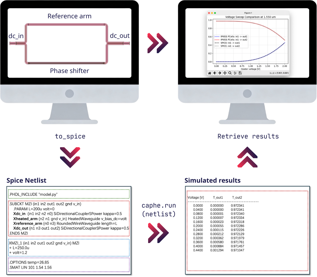
SPICE-based circuit simulation workflow.
This new workflow brings several benefits:
- Reproducible simulation input – Rerun simulations at any time from a SPICE file without rebuilding the circuit in IPKISS code.
- Decoupled simulation runtime – Run simulations independently of the IPKISS runtime, requiring only the Caphe simulator for repeated simulations.
- Improved debugging transparency – See exactly what is being simulated via the SPICE netlist, enabling easier setup and model debugging.
- What-if analysis – Modify netlist parameters after export (e.g., voltage biases) to perform sweeps and simulations under different conditions.
- EDA interoperability – Leverage SPICE as a standard format in the EDA ecosystem, allowing for better integration with other tools.
Check out "Running circuit simulations" for the API documentation and "A SPICE-Based Simulation Workflow in IPKISS” in the sample gallery.
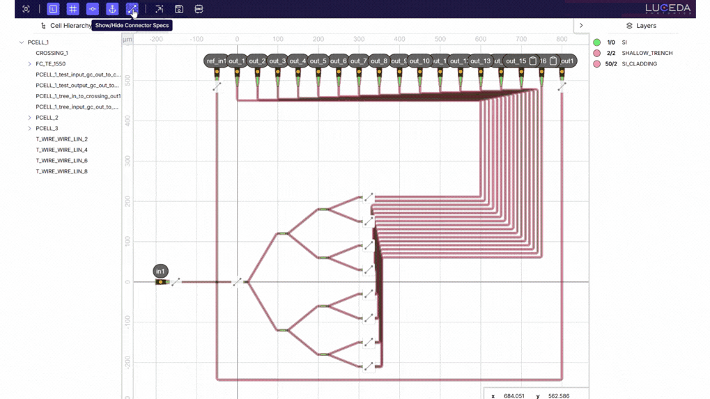
4. Visual P&R Assistance – Enhanced Visibility into Connectivity
With the enhancement to the Luceda Layout Visualizer, you can now visualize component connectivity within PIC layouts, simplifying the debugging of complex routing and making it easier to iterate on your circuit designs. When visualizing a PCell in the Luceda Layout Visualizer, connectors are clearly identified with a connector icon. Designers can click this icon to interactively inspect the connector’s control points and visualize exactly which reference point or coordinate system they are defined against.
Ready to bring verification closer to design?
Visit your Luceda Customer Portal, download Luceda 2026.03 today, and start designing your PICs with confidence from layout to fabrication!