
Ghent, Belgium - September 24, 2025
Luceda Photonics is proud to announce the release of the Luceda Photonics Design Platform 2025.09, delivering powerful new tools and workflow improvements to empower PIC designers worldwide. This release introduces the new interactive S-matrix Visualizer, enhancements to the Luceda Circuit Analyzer, a brand-new LVS (Layout vs Schematic) flow, major updates to the layout visualization and placement & routing (P&R) flow, and a new PDK layer creation process.
Key Highlights:
1. Interactive S-matrix Visualizer: Explore and Share Simulation Results
With the new Luceda S-matrix Visualizer, designers can now inspect and share frequency-domain simulation results.
- Select different port pairs, toggle linear/logarithmic scales, and customize plot styles.
- Export plots as static images or interactive HTML files that remain explorable when shared with colleagues.
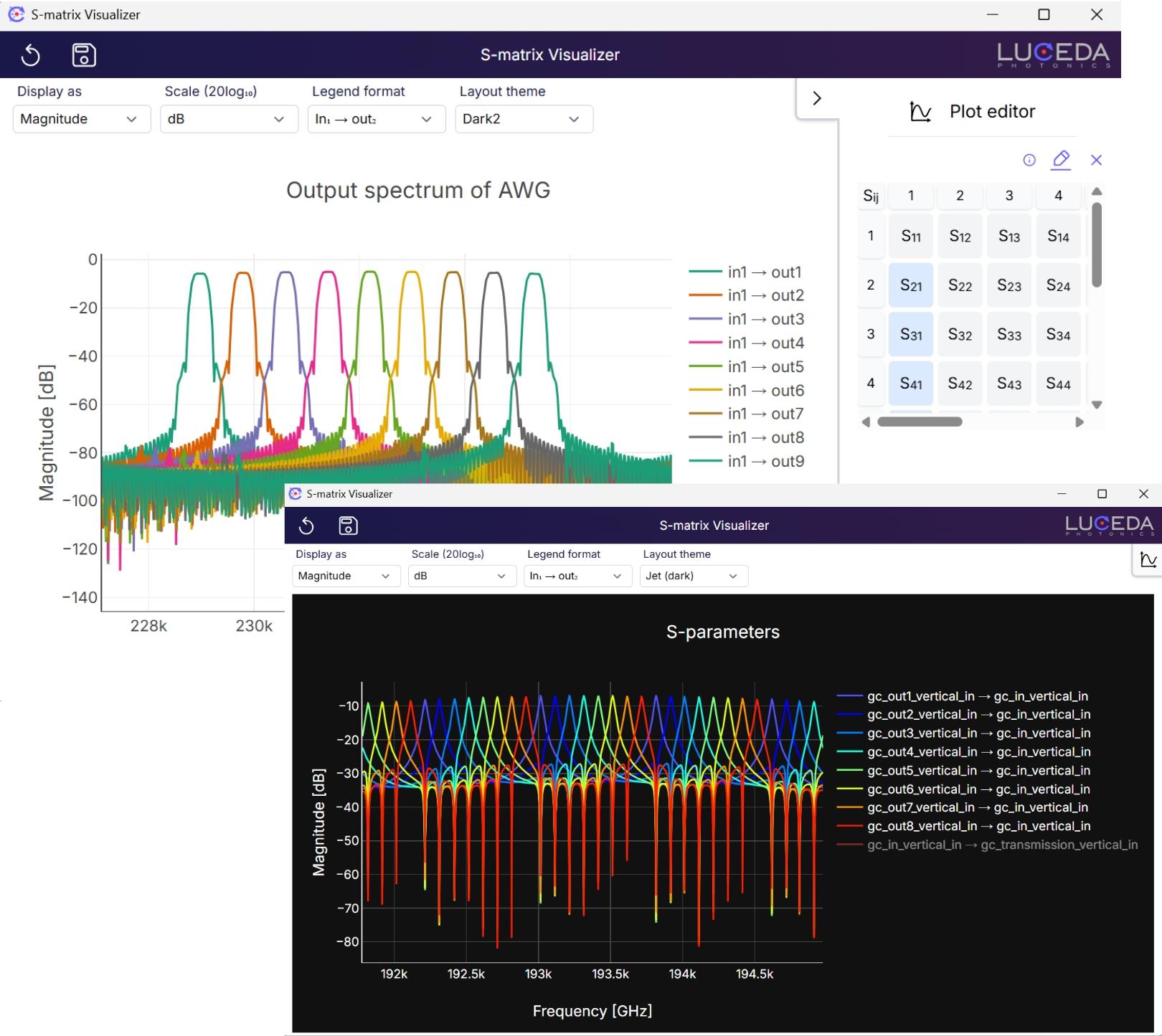 New S-matrix Visualizer
2. Enhanced SDL & New LVS Flow: Verify your design intent and implementation with Luceda IPKISS
Luceda IPKISS combines the strengths of schematic-driven and code-driven design flows. Designers can start from a golden schematic, simulate the circuit, and automatically generate and refine code to produce a GDS layout. From any finalized GDS layout, a schematic can be extracted, simulated, and verified against the original golden schematic to ensure full design consistency.
Get step-by-step guidance in the new tutorial on Luceda Academy: Layout versus Schematic (LVS)
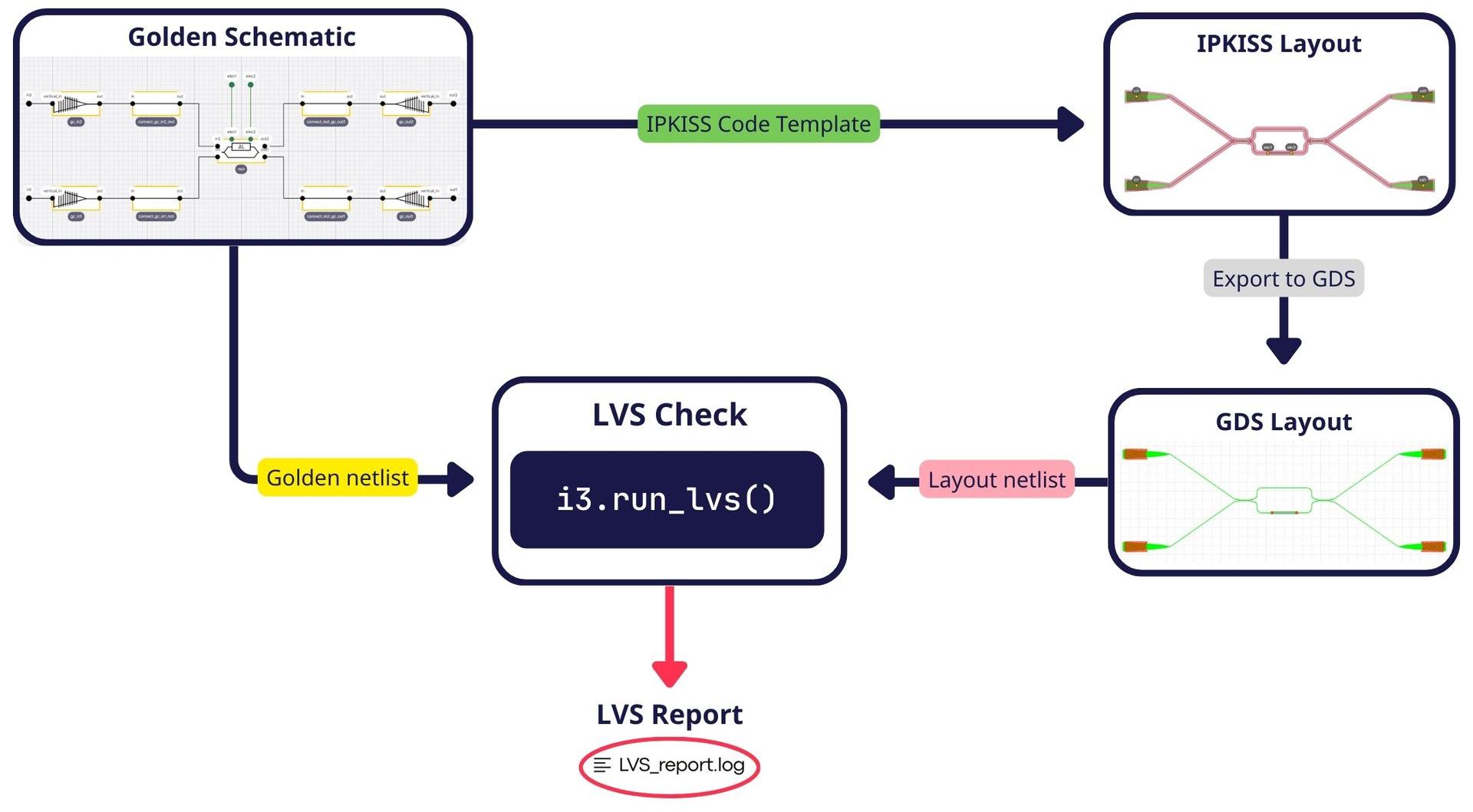
LVS flow in Luceda IPKISS
3. Better Control of Circuit Analyzer in IPKISS Canvas
Designers can now control Circuit Analyzer directly from IPKISS Canvas, helping them simplify and optimize the PIC design workflow.
- Define a schematic in IPKISS Canvas directly or extract it from a layout.
- Configure simulations and simulation corners.
- Simulate the circuit's behavior, including variations from nominal behaviour.
- Visualize simulation results directly in the improved visualizer.
- Iterate on the schematic and simulation parameters to rapidly develop insights into the behavior of the design.
4. New Circuit Analyzer Resources on Luceda Academy to Help You Get Started Easily
- New demonstrations - Location-Aware Variability Analysis and Corner Analysis.
- New examples in the sample gallery - Location Aware Variability Analysis of a Demultiplexer and Corner and Power Budget Analysis of MUX Devices.
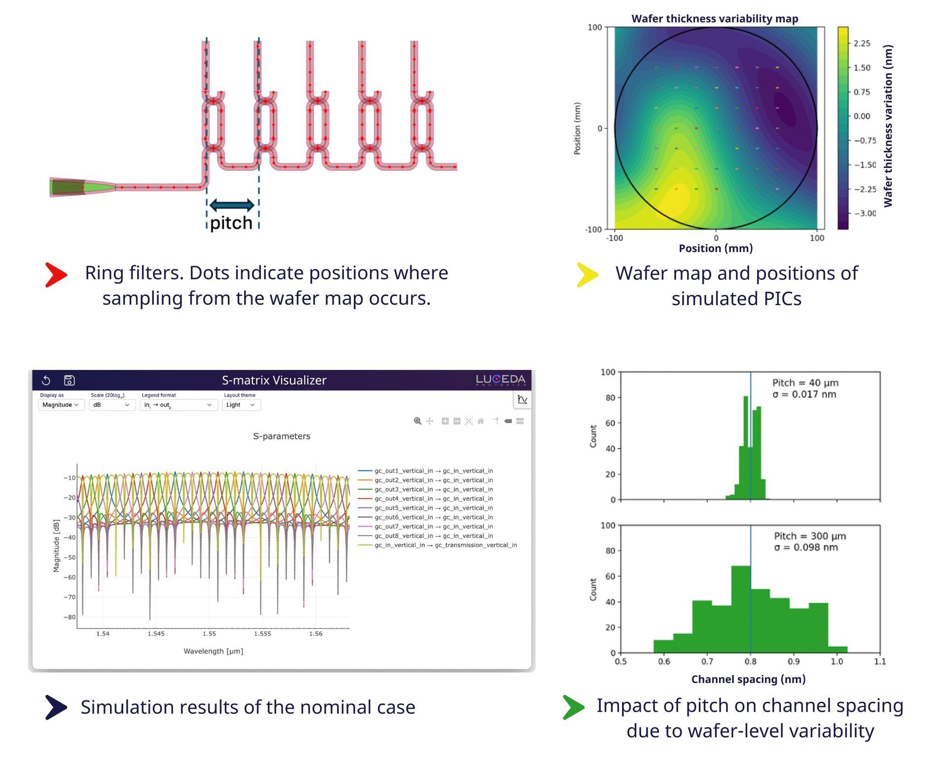 Example on Location-Aware Variability Analysis - impact of the pitch between rings on the channel spacing variability
5. Detect and Visualize DRC Violations Easily
With the updated Luceda Layout Visualizer, Luceda IPKISS makes
it easier to detect and visualize common DRC errors, such as sharp angles and layer
overlaps.
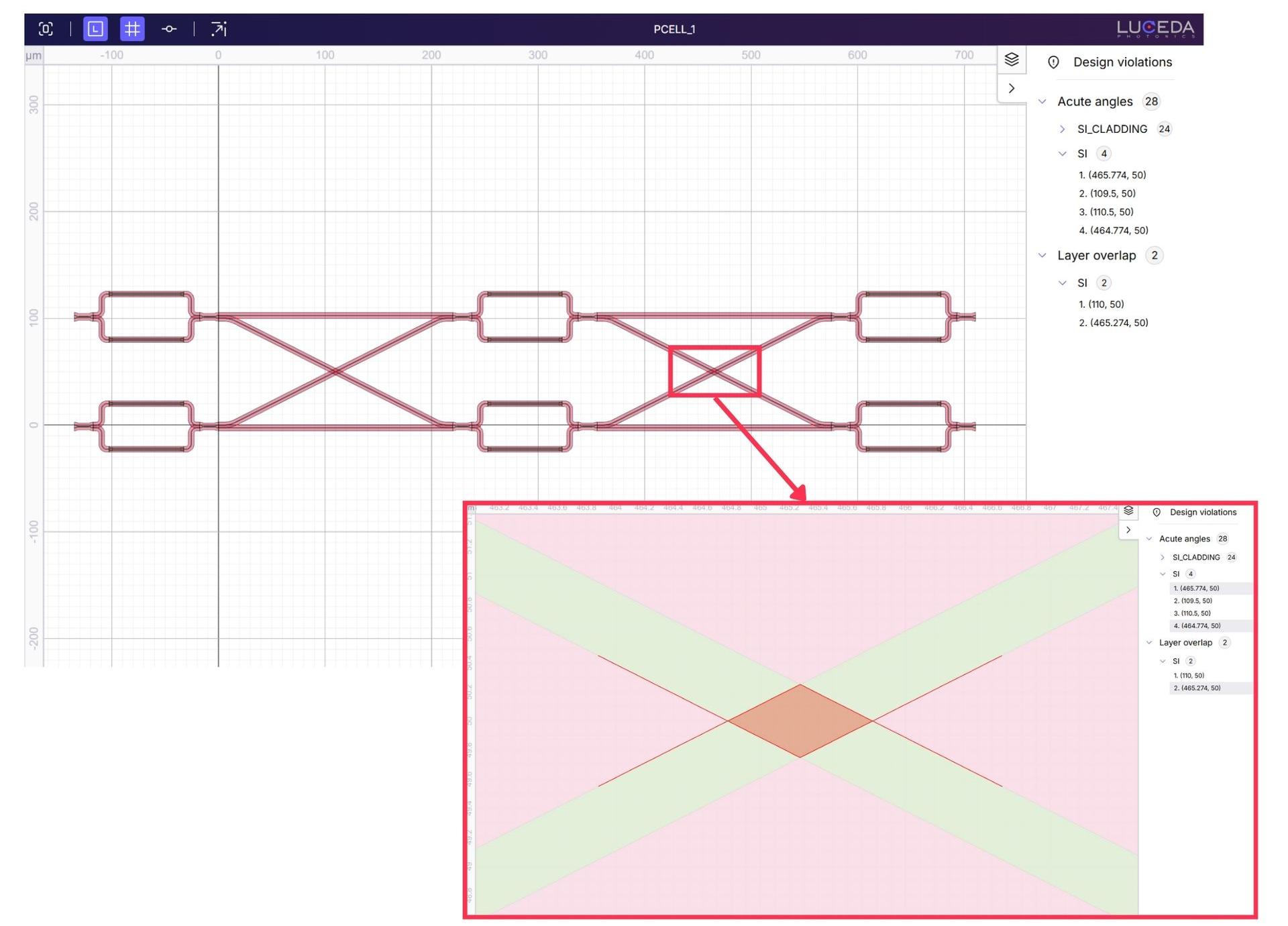
Detecting and visualizing acute angles and layer overlaps
6. Improved Layout Visualization for Faster Iterations
The updated Luceda Layout Visualizer provides a smoother and more immersive workflow:
- Multiple “.visualize( )” calls now open as tabs in one window.
- Re-running a script now reloads the view in its tab instead of opening a new window.
-
Instance and port names can now be easily inspected and copied for direct use in your code, streamlining placement and routing (P&R).
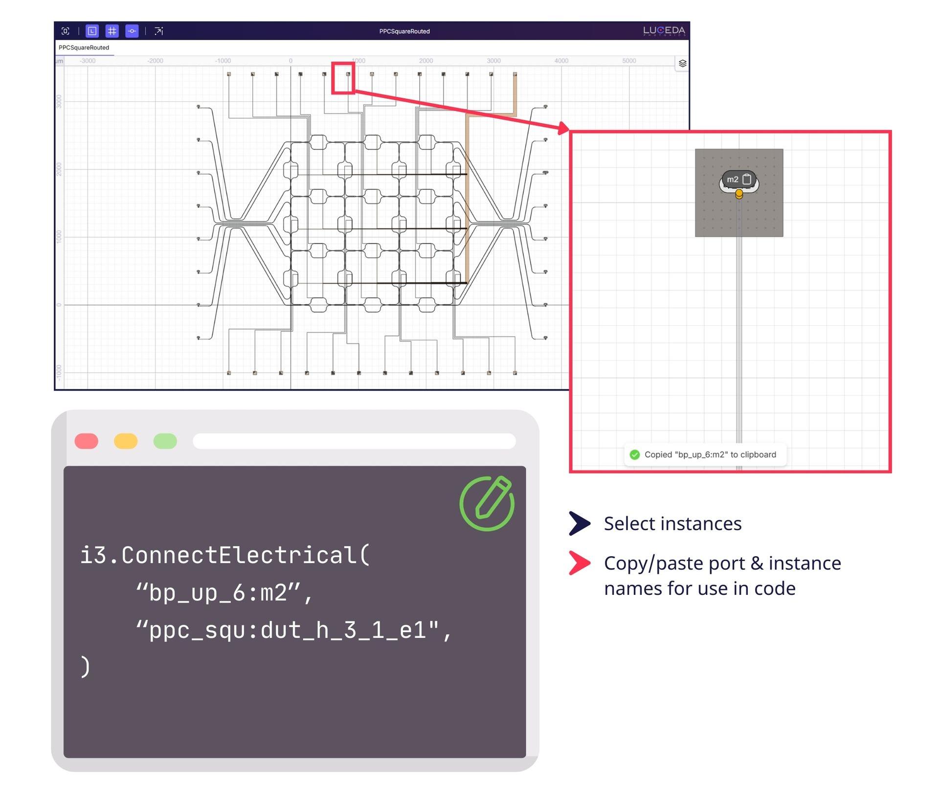
Interacting with instances and ports in an IPKISS Layout
7. New Placement & Routing Features
- Electrical routing with 45-degree corners: Designers can now add 45-degree corners to 90-degree bends in electrical traces, helping to reduce footprint, improve current density uniformity, and enhance fabrication yield.
- New cardinal anchors: Four default cardinal anchors (CN, CS, CE, CW) are now automatically available on every cell for P&R references. See Symbols for more information.
-
Custom
anchors: Expand the existing anchors with custom anchors for additional reference points in your designs. These custom anchors can be used in placement and routing in the same manner as the existing anchors, giving designers greater flexibility and control.

Electrical connector with 45-degree corners
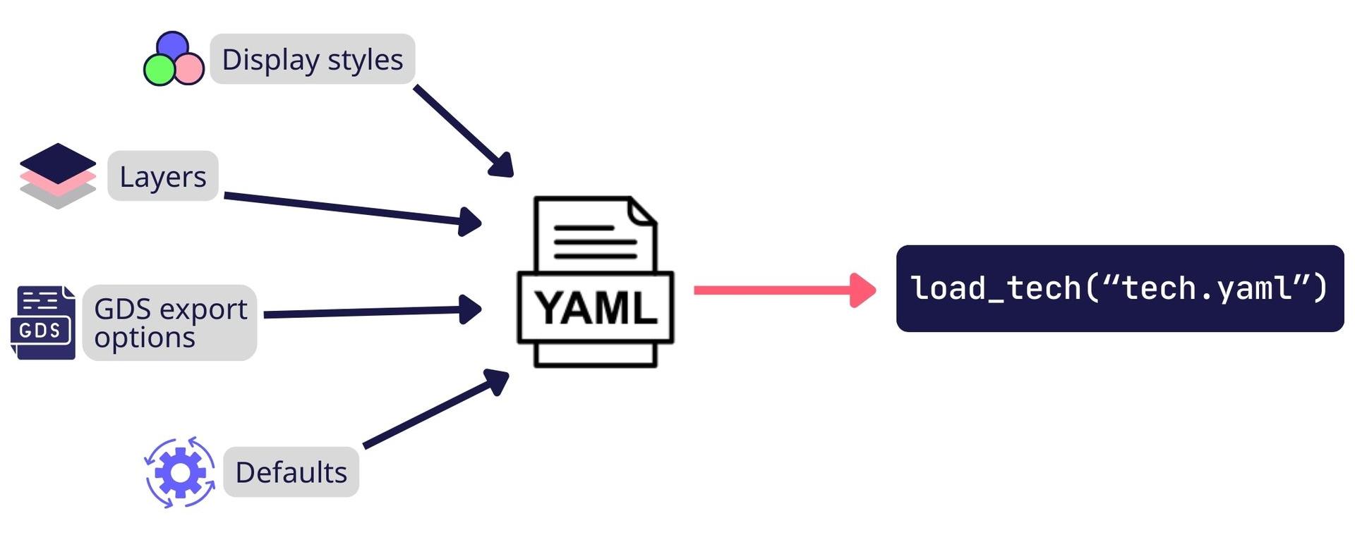
8. Simplified PDK Layer Creation Flow
Defining PDK layers is now simpler: all settings are in a single, human-readable tech.yaml file, with less code, making the initial PDK setup faster. For more information, check out the tutorial here: PDK structure
Download Luceda Photonics Design Platform 2025.09 from your Customer Portal and experience the enhanced PIC design capabilities!