
Dendermonde, Belgium - May 7, 2024
Luceda Photonics Design Platform 3.12 brings to you another round of significant improvements in the design of photonic integrated circuits (PICs). This release includes significant advancements in PIC placement and routing, introducing more features to enable obstacle avoidance and electrical bundle routing, alongside notable additions in tape-out preparation and circuit simulation.
More powerful and simple Placement & Routing
You ask, we deliver! With our upgraded P&R engine, you can create your PIC designs in a simpler, more compact way. The goal is simple: achieve more with less code!
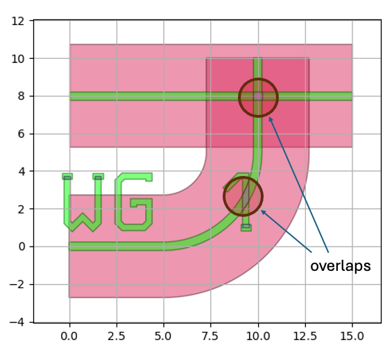
Avoid keep-out areas and easily control electrical and optical routing. Now, all instances come equipped with anchors alongside their ports. These anchors can be referenced during placement and routing, making it simple to define relationships between instances or routes within your circuit. This gives you more power and flexibility to avoid other devices or specific areas of your circuit, all without the need for manual calculations.
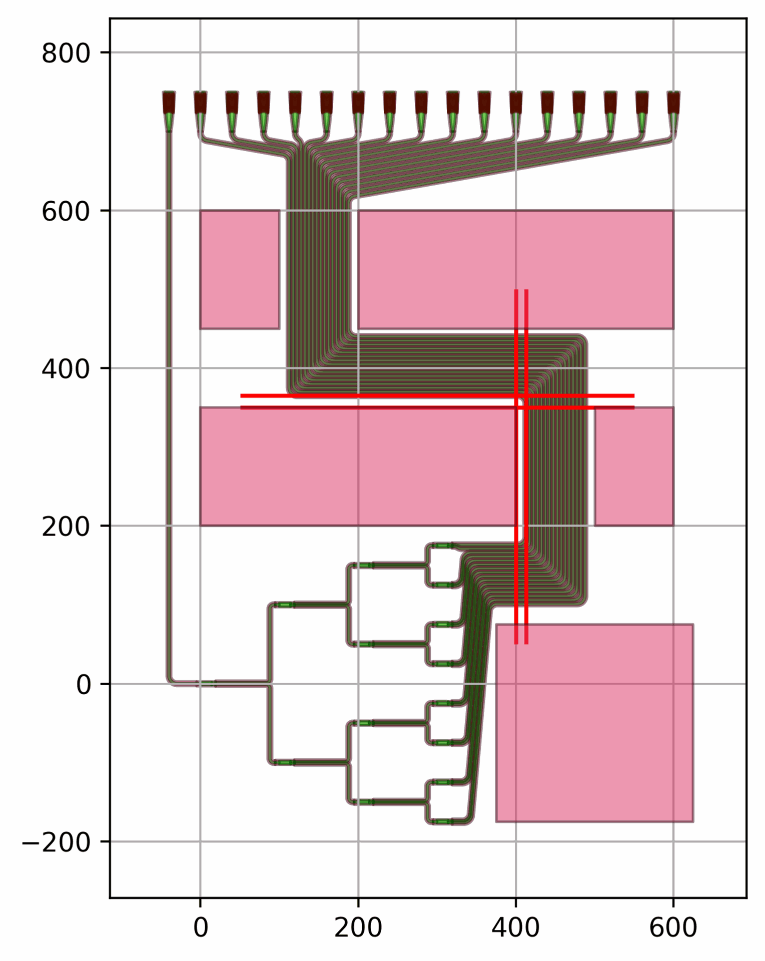
Additionally, the new electrical bundle connector further automates the electrical routing processes, enhancing your overall design efficiency. 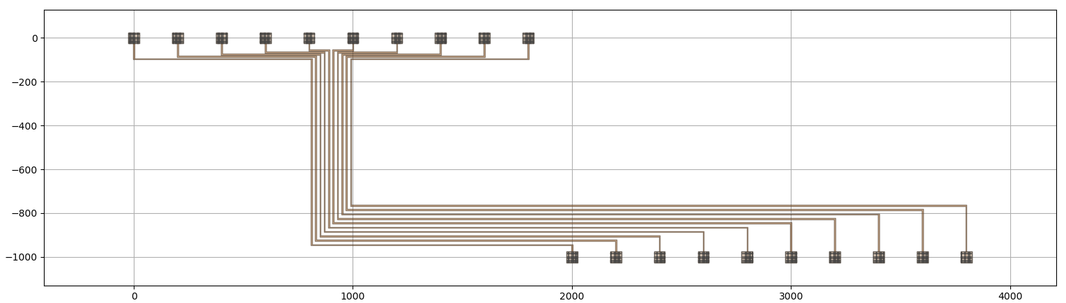
Tape-out preparation
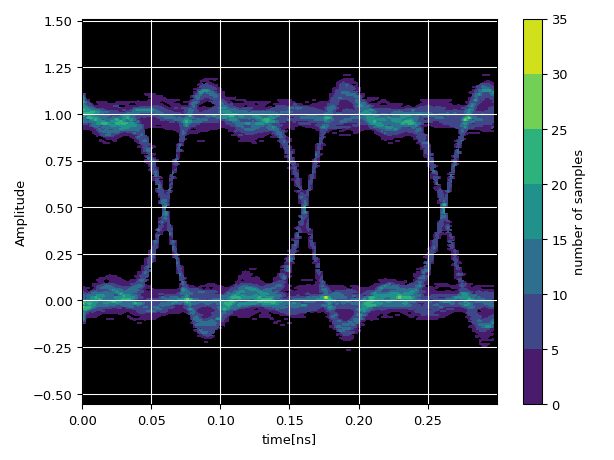
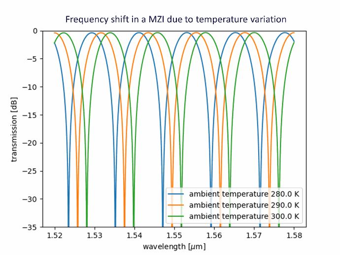
Temperature models and better simulation visualization
With the addition of temperature-dependent circuit simulations and advanced visualization routines for frequency and time domain results, such as eye diagrams, the IPKISS Caphe circuit simulator offers expanded capabilities for design analysis and provides designers with deeper insights into circuit simulation results, empowering them to make informed decisions throughout the design process.
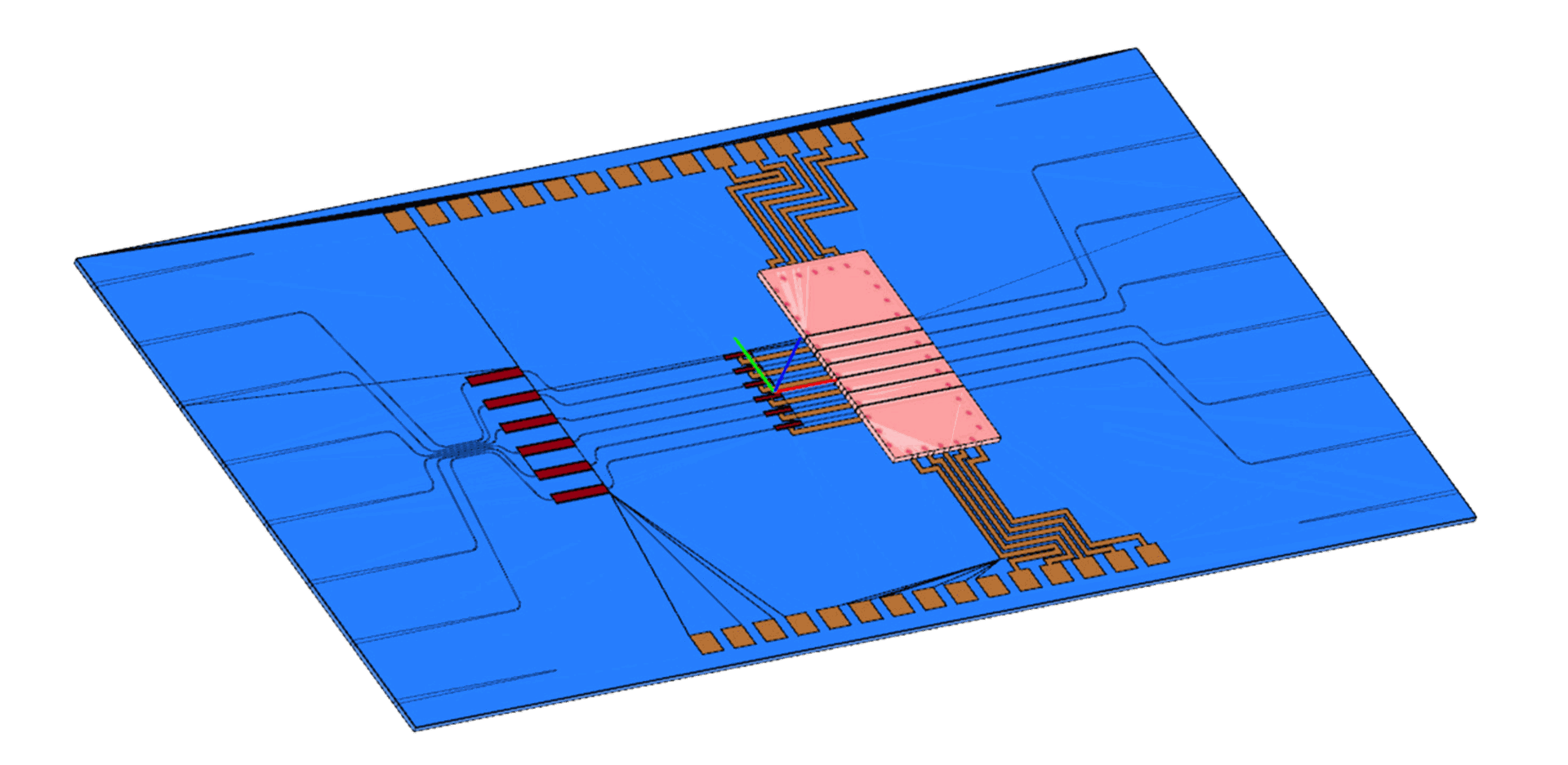
Export to standard 3D formats
All of these features work with over 30 supported foundry design kits (PDKs, ADKs and TDKs).
Don’t miss the chance to explore Luceda’s latest features using the tutorials available on Luceda Academy. Head over to your Luceda Customer Portal and download the latest Luceda 3.12!