Luceda E/O Co-Design Integration for Cadence
Accelerate your electro-optical IC development with Luceda Co-Design integration for Cadence, enabling a seamless workflow from photonic synthesis to physical and functional verification. By bridging Luceda’s Python-driven photonic synthesis with Cadence’s gold-standard EPDA ecosystem, this integration eliminates manual transfer errors and reduces time-to-market for next-generation interconnects.
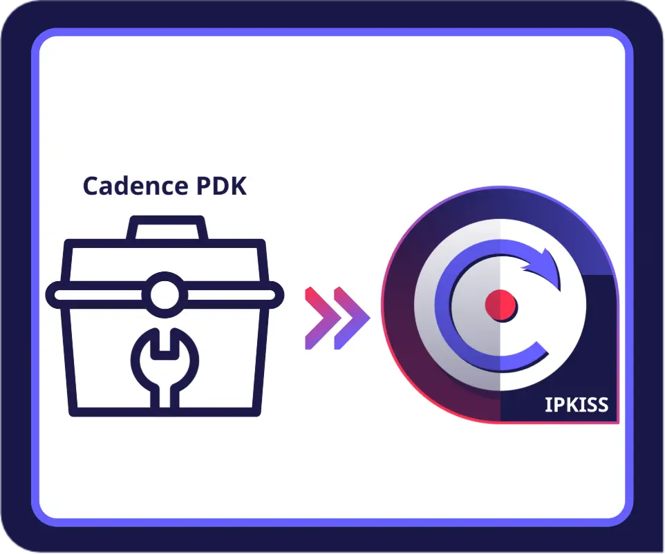
Use native Cadence PDK cells to directly implement the IPKISS Layout.
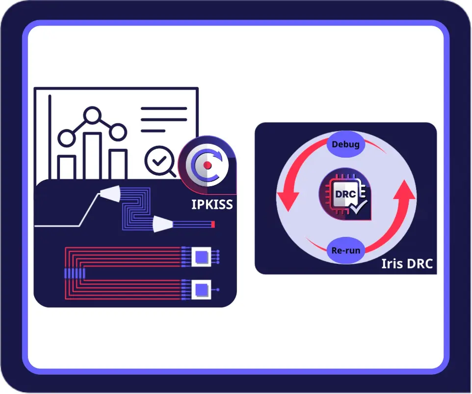
Leverage Luceda’s full curvilinear design capabilities, as well as verification with Iris DRC.
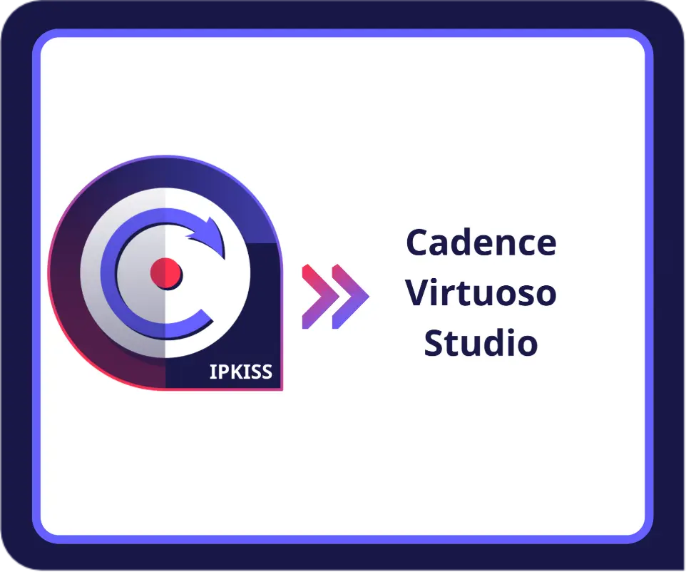
Export from IPKISS to the Cadence Virtuoso environment, with 1:1 cell & metadata matching.
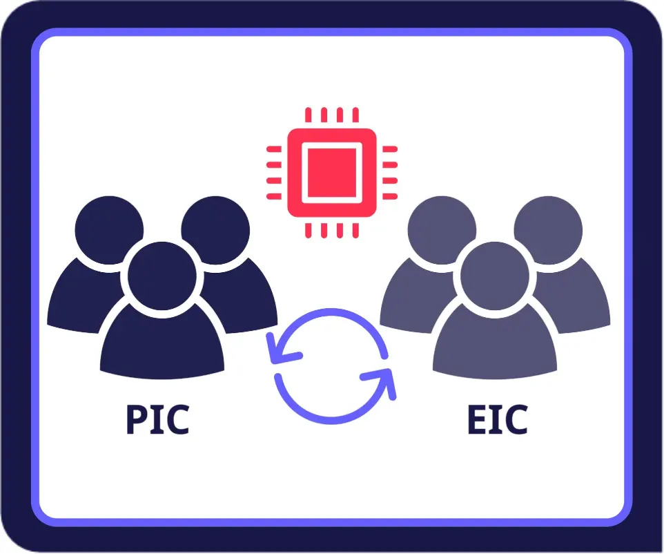
Align PIC & EIC design teams to co-design in lockstep.
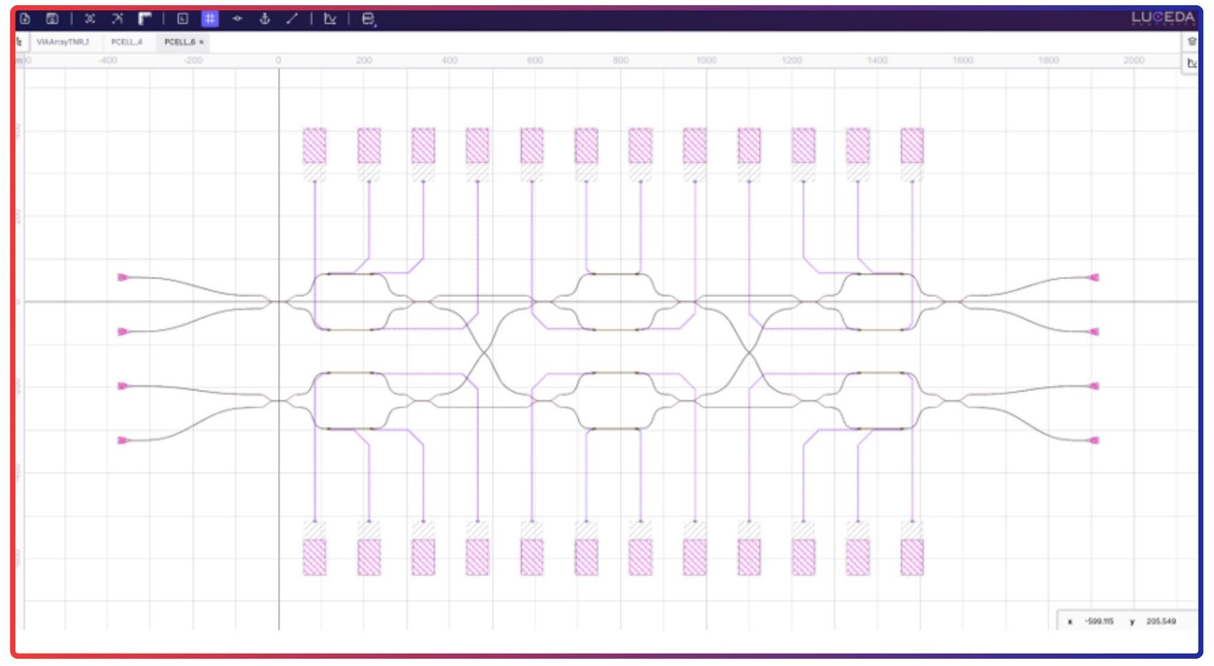
Switch layout in Luceda IPKISS, leveraging Luceda's specialized photonic synthesis.
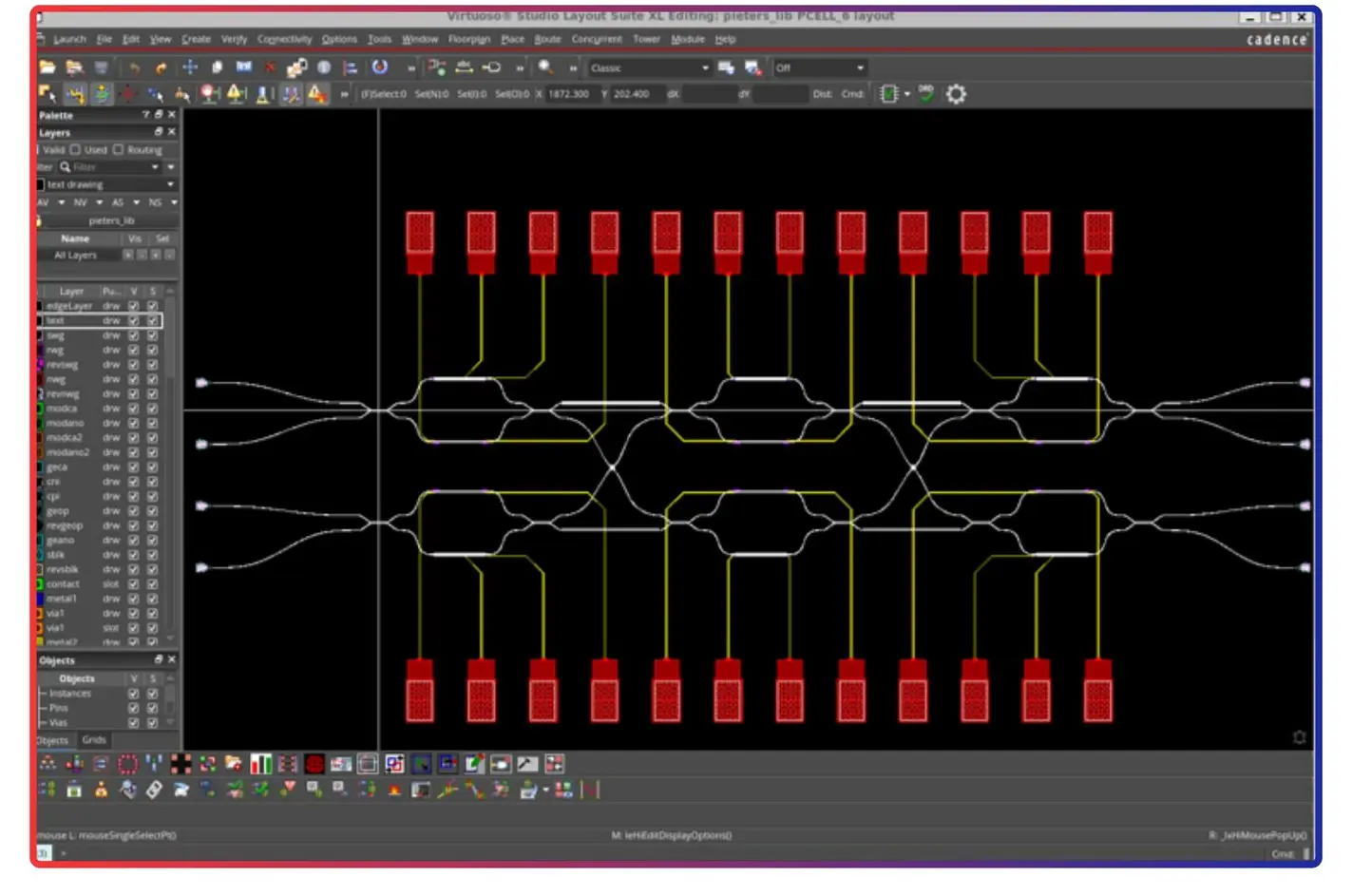
Exported Layout to Cadence Virtuoso Studio maintaining PDK cell mapping and metadata.
Pre-register for our Upcoming Webinar
Pre-register now and be the first to know when registration opens
for our upcoming webinar on Luceda E/O Co-Design Integration for Cadence.
About this product
The Luceda E/O Co-Design Integration for Cadence links the Luceda Photonics Design Platform with Cadence’s gold-standard EPDA ecosystem. Engineered for fabless PIC design teams building next-generation high-performance interconnects and for foundries, it delivers an automated bridge between Luceda’s specialized Python-driven photonic design synthesis to Cadence’s Virtuoso Studio for electro-optical system integration.
By eliminating traditionally isolated workflows and fragile manual transfers, the Luceda E/O Co-Design Integration for Cadence enables EIC and PIC engineering teams to work in lockstep. Photonic design teams leverage Luceda’s specialized layout, place-and-route, synthesis, and simulation capabilities while maintaining native compatibility with Cadence Virtuoso Studio and Spectre Simulation Platforms.
Ultimately, the Luceda E/O Co-Design Integration for Cadence provides an open, verification-backed environment that ensures first-time-right silicon production, transforming complex PIC-enabled technologies into market-ready interconnect solutions.
Benefits
For PIC Designers
- Eliminate manual file transfer errors and ad-hoc scripting through automated, 1:1 component and parameter mapping between Luceda and Cadence environments, accelerating time-to-market.
- Identify and resolve optical-specific design rule violations early in Luceda before initiating final full verification in the Cadence environment.
- Leverage a powerful workflow offering specialized PIC design and analysis capabilities (including curved, all-angle specification-based photonic placement & routing and fast functional validation) without sacrificing compatibility with standard CMOS/EDA design tools.
- Work in a highly flexible, open EPDA alternative instead of closed, single-vendor proprietary design ecosystems.
For EIC Designers
- Easily communicate and collaborate with the PIC design team within your team’s preferred design environment.
- Provide layout requirements and constraints that can be imported and used directly in the PIC team’s preferred design environment.
- Effortlessly combine the PIC design with the EIC design and prepare for tape-out, ensuring the layout is fully compatible with Cadence verification routines from the start.
For Foundries
- Drastically reduce the engineering hours typically required to build, validate, and maintain separate, disjointed PDKs for different design platforms.
- Effortlessly translate PDKs between Cadence and Luceda to expand your addressable designer market and customer base.
Current Core Features
Cadence PDK Import & 1:1 Mapping:
- Import Cadence PDKs or custom libraries directly into Luceda with full 1:1 parametric mapping of cells, parameters, and metadata.
- Synthesize and build complex photonic circuit designs within Luceda using native Cadence PDK components.
Bi-Directional Design Export & IP Generation:
- Export completed PIC designs back to the Cadence environment with lossless 1:1 parametric mapping of cells, parameters, and metadata.
- Create advanced PIC IP in Luceda (such as specialized AWGs via AWG Designer) and effortlessly transfer them to the Cadence environment to complete your circuit.
Constraint-Aware PIC Layout:
- Import layout constraints directly from the Electronic Integrated Circuit (EIC) layout.
- Account for physical, spatial, and electrical constraints during PIC layout implementation inside Luceda to ensure error-free electro-optical co-design.
Multi-Stage Electro-Optical Verification:
- Photonic DRC: Catch and resolve design rule violations early using Iris DRC directly inside Luceda.
- System Verification: Execute Layout Versus Schematic (LVS) and Check Against Source (CAS) within the Cadence environment to ensure full system functionality prior to tape-out.
Pre-register for our Upcoming Webinar
Pre-register now and be the first to know when registration opens
for our upcoming webinar on Luceda E/O Co-Design Integration for Cadence.
Interested in trying it out? Questions?