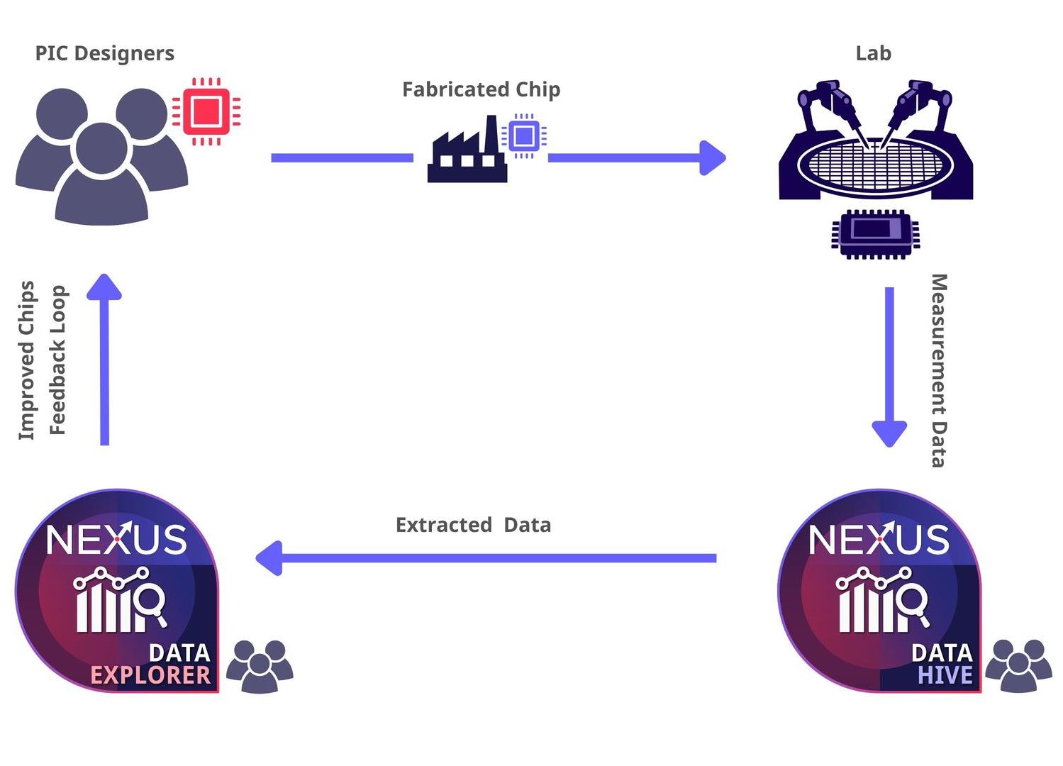
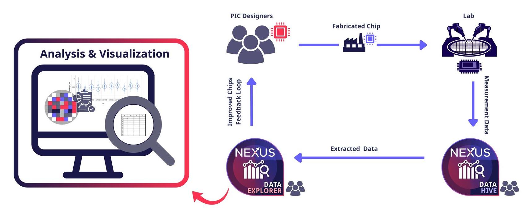
跳至内容

Nexus Data Explorer

Establish a permanent link between your design, the fab, and your circuit models. As part of the Nexus product line, Nexus Data Explorer provides a platform that can tailor advanced semiconductor data visualization and statistical analytics to reveal your PIC insights.

联系我们,申请试用


About  

Nexus is our product line designed for photonics data management and analytics, featuring Nexus Data Hive and Nexus Data Explorer. Nexus provides a standardized infrastructure for hardware-driven validation, helping you move away from fragmented scripts and manual data processing toward a fully integrated, automated data pipeline.

About Nexus Data Explorer

Nexus Data Explorer is a cross-platform (Windows & macOS) desktop application tailored for advanced semiconductor data visualization and statistical analytics. It serves as a core component of our mission to provide a continuous design-to-silicon feedback loop, giving you total control over your photonics design flow. Engineered for PDK modeling specialists, process integration engineers, and PIC designers, it combines exceptional ease of use with robust semiconductor engineering analytics.


Featuring a fully open ecosystem and multi-source connectivity, Data Explorer allows teams to analyze wafer-level data without the need for complex, hard-to-maintain manual parsing scripts. Whether you are opening lightweight local files, connecting to live production databases, or streaming extracted data from our industry workhorse, Nexus Data Hive, the platform delivers the interactive dashboards and advanced statistical tools needed to turn raw measurements into reusable knowledge and drive informed decision-making.

Core Features

  • Open Ecosystem & Multi-Source Connectivity:
    • File-level Ingestion: Instantaneous parsing and low-latency local rendering of tabulated data streams (e.g., Excel, CSV files).
    • Direct Database Linking: Native, out-of-the-box adapters that connect directly to major relational and columnar production databases (MySQL, PostgreSQL, MariaDB, ClickHouse, etc.).

  • Interactive Wafer Mapping: Generates real-time, interactive wafer maps supporting advanced spatial correlation analytics, critical dimension (CD) uniformity tracing, and fabrication defect distribution plotting.

  • Statistical Process Control (SPC) & Process Drift Detection: 
    • Enables robust cross-lot and cross-wafer statistical alignment, multi-dataset overlay comparisons, and historical trend monitoring.

    • Captures fabrication process drift at an early stage, outputting calibrated empirical boundary datasets to feed compact models, corner analysis, and advanced yield simulations.

Benefits

  • Start instantly with a quick setup and explore your existing data in minutes with Data Explorer, immediately generating PIC insights.

  • Accelerate engineering decision-making through interactive wafer-level visualization, statistical analysis, and automated reporting tools.

  • Eliminate dependency on fragile, manually handled scripts by providing a centralized and standardized analytics environment for photonic data validation.

  • Improve model quality and yield learning by establishing a direct feedback loop between silicon measurements, design data, and process monitoring.
  • Bridge the gap between engineering and leadership by easily generating professional presentations (e.g., PowerPoint) without requiring managers to run Python or Jupyter notebooks.

如果你感兴趣或仍有疑问,欢迎: