Module
Luceda AWG Designer
For photonic IC designers who enjoy ease-of-use and flexibility, the Luceda AWG Designer provides an integrated design environment to create manufacturable AWGs with a press-of-the-button flow.

About this module
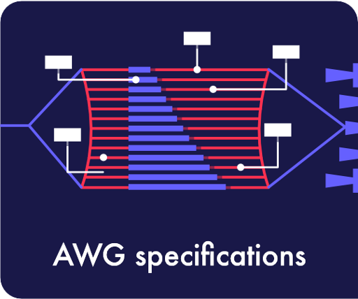
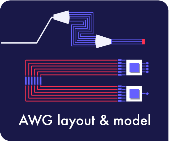
The Luceda AWG Designer is a Luceda module built on top of IPKISS that provides an integrated design environment to design Arrayed Waveguide Gratings (AWGs) from high-level specifications to manufacturable AWG layouts, offering expertise , assistance and control across all design stages:
-
AWG high-level specifications
-
AWG physical synthesis
-
Simulation and verification
-
DRC-clean layout generation
The Luceda AWG Designer enables optimization across all stages of the design flow while having a press-the-button flow to a manufacturable layout.
Each step of the process can be customized to suit specific requirements in terms of layout or simulation.
The final AWG design can be used within the Luceda Photonics Design Platform to complete the chip design and prepare for tape-out.
PIC designer benefits
-
Easy layout and simulation in a single integrated design environment, using one standard language
-
Fully parametric and customizable design flow
-
AWG design validation using analysis functions built into IPKISS
-
DRC-clean layout with IPKISS layout functionalities
-
Supported Luceda PDKs: AMF, Tower Semiconductor, Ligentec AN150, Ligentec AN800, imec iSiPP50G, imec BioPIX, CompoundTek, IMECAS
Support for other PDKs can be added upon request
-
Expert design support